IEEE
IEEE Home Search IEEE Shop Web Account Contact IEEE
Membership Publications/Services Services Standards Conferences Careers/Jobs

"Copper Die Bumps (First Level Interconnect) and Low-K Dielectrics in 65nm High Volume Manufacturing"
-- Dr. Andrew Yeoh, Logic Technology Development, Intel Corporation (Oregon)

Thursday, October 26, 2006
  • Buffet lunch served from 11:45 - 12:15 ($15 if reserved by Oct 23; $20 at door; vegetarian available); presentation at 12:15.
    If you like this topic, please see a follow-on talk we're holding on November 8th!


    Ramada Inn
  • 1217 Wildwood Ave (Fwy 101 frontage road, between Lawrence Expressway and Great America Parkway), Sunnyvale, (800) 888-3899 -- see map.

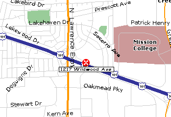
    PLEASE RESERVE IN ADVANCE --

  • If you pay using our PayPal link, you are automatically registered for the lunch and meeting
  • Otherwise, for lunch and meeting, pre-register by email to John Jackson, Analog Devices
    OVERVIEW:
    The benefits of copper die-side bumps for flip chip application are well known and have been sought for more than a decade. However, the introduction of fragile low-k interlayer dielectrics (ILD's) into back end interconnect architectures have made integrating copper bumps challenging, primarily due to low-k ILD cracks and delamination. For the 65nm technology node, Intel has successfully incorporated copper die-side bumps mated to eutectic tin-lead (SnPb) package-side bumps in high volume manufacturing (HVM). Advantages of using copper die bumps include lowering the bump CD floor, continued scaling of passivation openings that is driven by silicon interconnect line widths, a drastically simplified underbump metallization scheme, and extensions to higher I/O densities.
    With copper bumps, underbump metallization (UBM) now functions solely as an adhesive layer for the die-side bump, as the bump and silicon interconnect metals are identical. The barrier requirements of the UBM stack are eliminated since the highly reactive tin (Sn) constituent from the package-side solder is naturally isolated from the die-level copper interconnects by the die bump. Copper also brings a new geometry to the first level interconnect (FLI), where non-reflowed columns replace the familiar mushroom bumps that are reflowed into spheres. Eliminating die bump reflow simplifies the fab process flow in addition to enabling higher bump count per unit area.
    Integrating copper bumps requires added measures in the silicon architecture as the stiffer metal more directly transmits chip-attach stresses into the die when compared to SnPb. Assembly and reliability results that demonstrate the robustness of the overall architecture will be discussed. Fracture-mechanics-based modeling supports the empirical data and estimates a sizeable stress reduction within the low-k layers from utilizing SiO2.
    Enabling copper bumps brings to the table significant electrical benefits to design, scaling, and fabrication flow simplification. Beginning with the 65nm technology and incrementally going forward, each improvement that copper die bumps allow will be realized.

    Speaker Biography
    Dr. Andrew Yeoh has been at Intel Corporation for 9 years. He is presently Integration Group Leader for the passivation/C4/assembly area in the 65nm and 32nm technology nodes at Intel's Logic Technology Development division located in Hillsboro, Oregon. In this role, Dr. Yeoh is responsible for developing the process integration of die-package I/O interconnects.
    Prior to joining the process integration group, Dr. Yeoh was a CMP module engineer responsible for process development in the areas of oxide, tungsten, and copper planarization.
    Dr. Yeoh received his PhD in Materials Science and Engineering from the University of Texas at Austin in 1995. His academic background is in the areas of tribology, electromagnetic propulsion, and non-ferrous metallurgy.


    If you are not on our Chapter's regular email distribution list for meeting anouncements, you can easily be added! Please send an Email to Paul Wesling and let me know if you'd like email distribution.


    SCV Chapter Home Page
    How to Join IEEE
    Contact our Chapter Chair
    CPMT Society Home Page
    IEEE Home Page
    Email to Webmaster
    Last updated on