|
|
|
|
|
 | ||
|
| ||
 Wednesday, June 13, 2007
| $25 -- Register & prepay for dinner in one step from your PayPal account or Credit/Debit Card! |
Ramada Inn
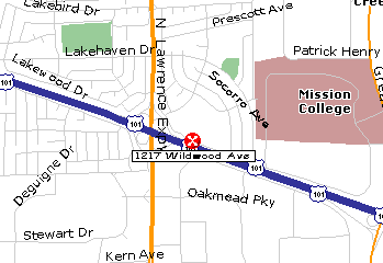
PLEASE RESERVE IN ADVANCE --
The challenge manufactures face when competing in the world marketplace is to offer a product that will meet all performance and functionality expectations without increasing product size or cost. Increased electronic functionality can be achieved through the development of more complex silicon integration but that route generally requires a great deal of capital resources and an excessive amount of time. Multiple-die package concepts are often proving superior to the system-on-chip alternative because it minimizes risk and has the potential for economically integrating several different but complementary functions. The information presented in this paper will review several package-on-package configurations and introduce a new packaging technology. A non-solder ball package, called "MicroContact", is based on a new substrate fabrication process developed to improve IC package density and circuit routing efficiency. In addition, the basic MicroContact package assembly methodology will be described and examples of high density stacked memory and mixed function variations shown. We will discuss the MicroContact effect on pitch, socketless testing, low profile, and reliability especially on lead free drop test.
Dr. Haba received his bachelor's degree in solid state physics from the University of Bab-Ezouar, Algeria in 1980. He holds two master's degrees in applied physics, materials science and engineering from Stanford University, where he also earned a Ph.D. in materials science and engineering in 1988. Dr. Haba holds 85 U.S. patents, and over 130 worldwide patents and patent applications. He has authored numerous technical publications and has also participated in many conferences worldwide
|
SCV Chapter
Home Page |
How to Join IEEE |
Contact our Chapter Chair |
FF
| CPMT Society
Home Page |
IEEE Home Page |
Email
to Webmaster |
Last updated on