IEEE/CPMT Dinner Meeting, in the Santa Clara Valley:
High Volume Print Forming: Filling the Gap between Nano and 'Just-Plain-Miniature' Devices
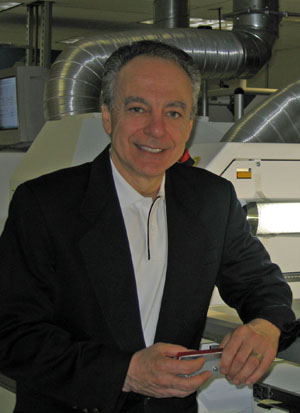
-- Arthur L. Chait, President, EoPlex Technologies
Presentation Slides: "Bridging the Gap Between 'Nano' and 'Just-Plain-Miniature' High Volume Print Forming " (2.5 MB PDF)
 Wednesday, February 13, 2008
Seated dinner served at 6:30
($25 if reserved by Feb. 10; $30 after & at door;
vegetarian available)
|
|
$25 -- Register & prepay for dinner in one step from your PayPal account or Credit/Debit Card!
|
Presentation (no cost) at 7:30.
Ramada Inn
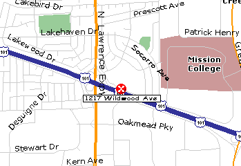
1217 Wildwood Ave (Fwy 101 frontage road, between Lawrence Expressway and Great America Parkway), Sunnyvale, (800) 888-3899 -- see map.
PLEASE RESERVE IN ADVANCE --
For dinner and/or meeting: by email to
Janis Karklins
Please reserve for "presentation-only", even if not attending the dinner.
- OVERVIEW:
-
A great deal of progress has been made in the field of nano and related "tiny" technologies. Unfortunately, the technology to link the tiny world to the macro world has not kept pace. The space between nano and macro is immense. At the nano end are self-assembling structures and semiconductor processes that deal in angstroms; and at the macro end are conventional machining and assembly techniques. Between these two extremes there is a gap where engineers struggle to make low-cost devices with complex 3-D structures containing multiple materials that are "Just Plain Miniature (JPM)."
This gap is often referred to as meso-scale and in this presentation we will consider a meso-scale of roughly 20 microns to 20 millimeters. A number of manufacturing technologies are used in this range including: thin film, lithography, etching, molding, embossing and micromachining. A very successful example is the application of semiconductor processing to create MEMs devices in silicon. MEMs airbag accelerometers and ink jet printer heads account for annual sales of several billion dollars per year.
However, semiconductor technology is not suitable for many other needs. Large, diverse markets exist for miniature devices that cannot be made with semiconductor technology and which require combinations of materials such as ceramics, metals and even polymers. The processes available to meet these needs are limited, costly and in some cases don't even exist. This presentation will review some of the existing technologies and then introduce a new technology call High Volume Print Forming (HVPF) that is able to fill an important portion of this gap.
HVPF is an additive manufacturing process that deposits layers in large panels to produce thousands of individual parts. It has some similarities to semiconductor processing, since HVPF can utilize conductors and insulators in the same layer. For example, it can produce a ceramic package with buried passive components and circuit conductors all at the same time. The technology can build temporary elements from fugitive materials to produce channels and open structures after heat processing. It has some similarities to rapid prototyping (RP) in that it builds parts from layers, but unlike RP the process works with conductors, dielectrics, passive components and is an actual manufacturing process not a model making technique like RP.
HVPF can be utilized with special versions of screen, stencil, offset and litho printing. Other methods like micro-dispensers, tape casting and jet printing can also be used for certain design elements. All of these techniques require proprietary "inks" to produce the ceramic, metal, catalyst or polymer features. These inks must print to high tolerance, bond where required, set quickly during the build and then decompose to the final material such as metals or ceramics. At the same time, the thermal properties of the materials must be adjusted to accommodate shrinkage, thermal expansion and other parameters.
This talk will discuss the technology and describe applications including: cell phone antennas, energy harvesters to replace batteries, thermal management devices, and microreactors for use in fuel cells.
- Speaker Biography:
-
Arthur L. Chait joined EoPlex in 2002 and was elected Chairman of the Board in 2003. EoPlex is a Silicon Valley startup that utilizes new technology to manufacture low cost ceramic-metal components for miniature energy devices, sensors, fuel cells, pumps, packages, and circuits. Mr. Chait has raised two rounds of VC funding and the company is now backed by Draper Fisher Jurvetson, ATA Ventures, Labrador Ventures, and Draper Richards.
Prior to EoPlex, Mr. Chait was with Solectron (NYSE) as Senior VP Global Accounts where he had revenue responsibility of over $10 billion/year with customers including; IBM, Cisco, Dell, Apple, Ericsson, SUN, Nortel, Nokia, HP/Compaq, Motorola, and Lucent.
Mr. Chait’s prior experience also includes: GM Zitel (NASDAQ) where he created the software division; Senior VP at Stanford Research Institute with responsibility for 600 staff and all international offices; Booz Allen & Hamilton where he managed assignments in technology strategy for major OEMs; and Dresser/Halliburton where he was a research director in advanced materials.
Mr. Chait holds an MBA from the University of Pittsburgh and a BS in Materials Engineering from Rutgers University and was also awarded the Steinmetz Medal from GE.
If you are not on our Chapter's regular email distribution list
for meeting anouncements, you can easily be added!
Place yourself on our email distribution list or send a request to
Paul Wesling.]
Last updated on
