|
|
|
|
|
 | ||
|
| ||
 Wednesday, May 14, 2008
| $25 -- Register & prepay for dinner in one step from your PayPal account or Credit/Debit Card! |
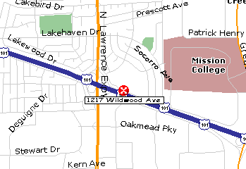
Ramada Inn
PLEASE RESERVE IN ADVANCE --
A concept for a high-performance module using build-up layers on copper is presented. Copper provides mechanical support, an electrical backplane, good thermal conductivity, and is impervious to water. Photolithographic processing can be performed on wafer-sized copper substrates using coaters and aligners (from Suss Microtec, for example). Stacked module configurations can be well-cooled, and have good test and rework capabilities.The ability to make compact assemblies with high silicon content spurs parallel development in the areas of cooling, testing, and rework. New test and cooling concepts will be described, looking towards automated assembly, test, and rework at the wafer level. Potential innovations in socketing and optical interfaces will also be briefly described.
A few observations about the materials aspect of copper-based electronic modules:
- A blade server of today comprises around 0.1% silicon and 55% air by volume. Only the silicon is doing useful work.
- Modern packaging can support around 20% silicon and 5% air if the twin problems of heat dissipation and testability can be solved.
- Copper is ~1600 times more thermally conductive than FR4 epoxy laminate.
- In terms of forming a barrier to water, 1 micron of copper is roughly equivalent to 1 centimeter of glass and to 100 centimeters of epoxy.
- Assuming 1 liter/min of cooling fluid, water can cool around 4,000 watts while air can cool only around 0.2 watts.
- Copper can be multi-functional in four dimensions: electrical conductivity for controlled impedance and shielding; thermal conductivity for heat spreading; low water permeability supporting integrated cooling channels; and good mechanical support.
The packaging strategies are supported by 12 new patent applications, some of which have issued.
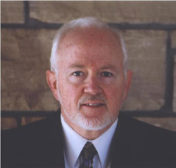
- Speaker Biography:
- Peter Salmon is a systems engineer and inventor. He has authored over 25 patents in the areas of electronic packaging, high-speed digital printers, and electrostatic motors and generators. His packaging patents include novel solutions to flip chip manufacture and assembly, advanced socket assemblies, a new functional test method at the board level, parallel testing of microprocessor wafers at full speed and full power, advanced copper substrates, and automated assembly test and rework at the wafer level. He holds a bachelor’s degree from Auckland University, New Zealand, and two graduate degrees from Northeastern University, all in Electrical Engineering.
|
SCV Chapter
Home Page |
How to Join IEEE |
Contact our Chapter Chair |
| CPMT Society
Home Page |
IEEE Home Page |
Email
to Webmaster |
Last updated on