IEEE/CPMT Luncheon Meeting, in the Santa Clara Valley:
"Electro-Optical Microscopy: Evolution in Component and Package-Level Inspection"
-- Andrew Kominek, Micro Analysis Group, Keyence Corporation
Presentation Slides: "Electro-Optical Microscopy: New Age of Inspection" by Andrew Kominek (1.5 MB PDF)
 Thursday, November 20, 2008
Registration at 11:30 AM; Buffet lunch served from 11:45 - 12:15
($15 if reserved by Nov. 17; $20 at door;
vegetarian available); presentation at 12:15.
|
|
Register & Prepay for lunch ($15) in one step from your PayPal account or Credit Card!
|
Ramada Inn
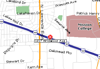
1217 Wildwood Ave (Fwy 101 frontage road, between Lawrence Expressway and Great America Parkway), Sunnyvale, (800) 888-3899 -- see map.
PLEASE RESERVE IN ADVANCE --
If you pay using our PayPal link, you are automatically registered for the lunch and meeting
Otherwise, for lunch and meeting, pre-register by email to
Ed Aoki, aoki.ed@gmail.com
- OVERVIEW:
-
This presentation introduces digital microscope technology and its application in semiconductor development, failure analysis, and quality control. The integration of rapidly advancing digital image processing with slowly improving optical microscopy has advanced the use of microscopy as a tool for the component, process and packaging engineer. Bridging of the two technologies has allowed for unprecedented inspection and image analysis capabilities. Advanced optics and software algorithms produce high resolution images with near-infinite depth-of-field; SEM-like images are the result. Post-processing of captured images allows the user to change point of view and to make critical measurements, as well as inserting comments and arrows.
I plan on having the equipment with me to demonstrate after the presentation. I think that would give a much better understanding as to the capabilities of this type of equipment. I can also image samples for the attendees should they choose to bring some.
- Speaker Biography
-
Andrew Kominek is a Sales Executive and Applications Engineer with the Micro Analysis Group at Keyence Corporation. He received his B.S.E.E. from the University of Texas at Austin in 2006 and has been responsible for marketing and supporting the Keyence digital microscope in the Bay Area for the past two years. During that time he has worked with numerous companies spanning a variety of industries, including automotive, semiconductor, medical device, defense, and more recently, solar.
His efforts have been a driving force in the penetration of the solar market and have resulted in nearly a threefold increase in sales to both medical device and semiconductor industries, with sales exceeding 2.5 million dollars over the past two years. He also secured the largest quantity microscope order in Keyence America history with one of the top semiconductor equipment suppliers in the world.
If you are not on our Chapter's regular email distribution list
for meeting anouncements, you can easily be added!
Place yourself on our email distribution list or send a request to
Paul Wesling.]
Last updated on
