IEEE
IEEE Home Search IEEE Shop Web Account Contact IEEE
Membership Publications/Services Services Standards Conferences Careers/Jobs

    MEMS and BioMEMS in Laminates
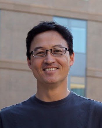
    -- Professor Mark Bachman, Dept. Electrical Engineering and Computer Science, University of California-Irvine

Presentation Slides: "MEMS and BioMEMS in Laminates" (1.3 MB PDF)

Thursday, October 24, 2013

  • Registration at 11:30 AM; Buffet lunch served from 11:45 - 12:15 ($15 if reserved by Oct. 22; $5 for fulltime students and currently unemployed; $5 more at door; vegetarian available; presentation (no cost) at 12:15.
    OVERVIEW:
        Post-semiconductor manufacturing processes (PSM), including packaging and printed circuit board (PCB) manufacturing, are now capable of producing trace widths of a few micrometers, high-aspect-ratio vias, three-dimensional constructions, and highly integrated systems in a single small package. Such PSM technology can in principle be used to manufacture micro electromechanical systems (MEMS) for sensing and actuation applications. Although MEMS are traditionally produced using silicon processes, the broad array of manufacturing approaches available in the packaging industry -- including lamination, lithography, etching, electroforming, machining, bonding, etc. -- and the large number of available materials such as polymers, ceramics, metals, etc., provides greater design freedom for producing functional microdevices. The results of such processes applied to fabricating small systems are heterogeneously integrated MEMS devices.
        In many cases laminated MEMS devices are more suited to their applications than their silicon counterparts, especially for applications such as biomedical, optical, and human sensing. Furthermore, such microdevices can be built with a high degree of integration, pre-packaged, and at low cost. Indeed, the PCB and packaging industries stand to benefit greatly by expanding their offerings beyond serving the semiconductor industry and developing their own devices and products. This talk illustrates that good-quality MEMS devices can be manufactured using packaging-style fabrication, particularly using stacks of laminates, and discusses some of the unique benefits of such devices. This "laminate MEMS" technology promises not only improved methods for manufacturing microdevices but also for heterogeneously integrating them with silicon microelectronics and other components into a single package.

    Speaker Biography:
        Professor Mark Bachman is a member of the faculty in Electrical Engineering and in Biomedical Engineering at the University of California, Irvine. He is Principal Investigator of a team of researchers and students in projects for DARPA, NSF, NIH, ARMY, UC Discovery, Calit2, and numerous companies. Projects include microfluidics, cellular arrays, MEMS devices, micro-acoustics, bioflexible micro devices, eHealth, and the human computer interface. Dr. Bachman's work develops technology solutions to problems in life sciences, environment, sensor systems, and micro-scale manufacturing. His specialty is integrated microsystems, where one uses micro-scale technology as part of an integrated technology solution.
        Mark received his Ph.D. in physics at the University of Texas in Austin. He has been active in research for MEMS, nanotechnology, and integrated microsystems for over 12 years. He is co-founder of UC Irvine's Integrated Nanosystems Research Facility (INRF), and UC Irvine's Bio-Organic Nanofabrication facility (BiON).


    If you are not on our Chapter's regular email distribution list for meeting anouncements, you can easily be added! Place yourself on our email distribution list or send a request to Paul Wesling.]


    SCV Chapter Home Page
    How to Join IEEE
    Contact our Chapter Chair
    CPMT Society Home Page
    IEEE Home Page
    Email to Webmaster
    Last updated on