 Technical
Committee
Technical
CommitteeNano Packaging
Technical
Committee
Nano Packaging
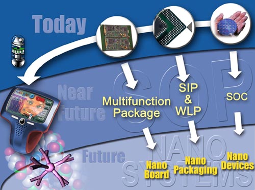
CPMT views nano-packaging and nano-systems integration to be its strategic mission. However, while there has been lot of nano focus from scientists in nanosciences leading to nano-devices, there has been very little nano-engineering into products.
The mission of this Technical Committee, therefore, is to promote nano-packaging and nano-systems engineering and integration, globally leading to nano-components and nano-systems.
• A nanometer is
1 billionth of a meter; the width of 10 hydrogen atoms.
• Engineers accept up to 100 nanometers as being “nanoscale.”
• Beyond silicon
for electronics
• Potential to unravel secrets of bio cell
• Superior electrical, mechanical, chemical, optical properties
• Electronics and
IT
• Heath care
• Environment protection
• Energy
• Anti-terrorism and homeland defense
The Nano Packaging Technical Committee aims to be involved in both nano-research and nano-education. Research dissemination is accomplished by means of global workshops and conferences. The education will be accomplished by means of publications, short courses, academic courses and books.
| Nano Package Design | Nano Power Sources |
| Nano Bio-Packaging | Nano Electro-Mechanical Systems (NEMS) |
| Nano Sensor Packaging | Nano Materials by Design |
| Nano Packaging Materials & Processes | Nanoscale Processes for Environmental Improvement |
| Nano Wafer Level Packaging | Energy Conversion Storage |
| Nano Dielectrics | Nanoscale Instrumentation and Metrology |
| Nano Capacitors | Nano Mechanics |
| Nano Fluidics | Nano Micro Transition |
| Nano Interconnections and Wiring | Nano Interfaces |
| Nano Thermal Science | Nano Measurements |
| Nano Optics & Optical Interconnections | Nano Packaging Lithography |
View our full list of members in the U.S.A., Europe and Asia
The committee meets once a year at ECTC and once a year either in Europe or in Asia . The scope of this committee includes influencing CPMT activities and publications in the area of Nano Packaging. This includes:
2nd
International Workshop on Nano & Bio-Electronics Packaging, March
22-23, 2005,
Grand Hyatt Hotel, Atlanta, Georgia, USA
Focus will be on Nano Photonics, Nano Imprint Processing, Nano Wafer
Level Packaging,
Nano Bio-Packaging, Nano Manufacturing, NEMS & Sensors, Nano
Materials &
Processes and Nano Fluidics.
Abstract Submissions:
Please send
title and 300-word abstract, electronically, to nbep@ee.gatech.edu
by October 15, 2004. Download
Call for Papers (PDF).
To Join the Nano TC
Anyone can be a participating member of one or more of the CPMT Society's TCs
without belonging to the IEEE; most of our TCs have a mailing list, a newsletter,
and a networking listing.
For more information, or to join our TC, send an email note or letter to:
Rao Tummala, TC Chair
Packaging Research Center, Georgia Tech
813 Ferst Drive, NW
Atlanta, GA 30332 USA
+1-404-894-9097
Last updated on
|| Send comments to
Reed Crouch.