Components, Packaging & Manufacturing Technology Society

IEEE/CPMT Dinner Meeting:

"IC Packaging Roadmaps" --
Dave Tovar, IPAC

Wednesday, December 13, 2000
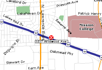
  • Seated dinner served at 6:30 ($20 if reserved before Nov. 5; $25 after & at door; vegetarian available)
  • Presentation (no cost) at 7:30.

    Ramada Inn

  • 1217 Wildwood Ave (Fwy 101 frontage road, between Lawrence Expressway and Great America Parkway), Sunnyvale, (800) 888-3899 -- see map.

    PLEASE RESERVE IN ADVANCE --

  • For dinner and/or meeting: by email to Tom Tarter
  • or call our CPMT hotline at 1-650-299-8898.
  • Please reserve for "presentation-only", even if not attending the dinner.

    OVERVIEW:
    Microminiaturization of microelectronic packages continues to be the leading limiting factor for advanced interconnect technologies worldwide. In addition, improved mechanical, electrical, and thermal characteristics allow the packages to be of better quality and reliability. In order to keep up with this very fast and exciting pace, the major assembly subcontractor houses have found it necessary to combine their research and development efforts either through the integration of internal departments/divisions or else by the establishment of business partnerships/alliances with key customers. In this manner, R&D efforts can proceed in a multiplexed fashion that will result in improved time-to-market of new customer product and, of course, lower prices.

    Orient Semiconductor Electronics, Ltd. (OSE) has joined forces with (IPAC) Integrated Packaging Assembly Corporation (IPAC). By combining research (OSE) and development (IPAC) forces, both companies now enjoy the benefits of supplying their domestic and foreign customers with fast and reliable microelectronic packages from substrate design to electrically tested drop-ship product. Development in advanced materials, improved manufacturability, tighter wire bond pitches, wire bonding to copper bond pads continue as usual on current assembled product. Recent package introductions in the area of advanced interconnects include:

    1. Stacked Die - Two and three memory die stacked on top of each other in a chip-scale package (CSP) format.
    2. Metal Lead Package (also known as QFN) - CSP with embedded leadframes, no leads
    3. Flip Chip (FC) - Single or multichip wireless packages intended for high performance or high leadcount packages.
    4. Wafer Scale Integration (WSI) - Fan-in designs from tight peripheral bond pad designs to more manageable area array formats through the use of an organic dielectric and a metallic interconnect.

    Speaker Biography:
    Dave Tovar holds an EP from Heidelberg University, Germany, a BS degree in Analytical Chemistry and an MS in Chemical Engineering from SJSU. A 25+ year veteran of the semiconductor industry, Dave has held engineering and managerial positions in R&D, manufacturing operations including materials, design, process, product engineering, electrical testing, failure analysis, and R&QA. He has worked at IBM, Fairchild, Qualidyne, National Semiconductor, SEEQ, VLSI Technologies, Synergy, GateField, Hyundai, ChipPac, PacTech, and is presently at IPAC.

    If you are not on our Chapter's regular email or FAX distribution list for meeting anouncements, you can easily be added! Please send an Email to Tom Tarter and let me know if you'd like email or FAX distribution. If you don't have Email, then please reply to 800 686-9366 (CPMT's 800 number), but please be advised that I would greatly prefer the Email route.


    SCV Chapter Home Page
    How to Join IEEE
    Contact our Chapter Chair
    CPMT Society Home Page
    IEEE Home Page
    Email to Webmaster
    Revised 22 August 2000